
Even before purchasing one, I asked myself, what additional settings the switches on the board may provide. This page exists to summarize my observations and results publically.
After some actualizations in the first three years the side remained unchanged for a long time. However, since there's still a lot of traffic, I've updated the page now - 6 years later - to a more modern layout, to add some missing informations, and - finally - an english version. Much of the page however is still outdated and will stay that way.
The translation is based on an automated translation with some manual cleanup, dont expect it to be perfect.
- The revisions
- The variations of the K6
- FSB clock settings
- Clock multiplicators
- Core voltages
- Processor clock
- IRQ management
- System monitoring and the fan
- Win98 and two monitors
- SCSI BIOS
- Known problems of the board
- Update of 2006
All my observations refer to the P5BV3+ revision A1, B5, c1 and to the K6XV3+/66 revision B1.
The board revision consists of a type identification (A, B,..) and the revision number (0.1.2...).
The only reliable source for this number is the inscription in the middle on the board, in the proximity of processor pin 1. The indication in the manual is not enough. DFI identifies the boards additionally on the basis a sticker on the outermost ISA plug.
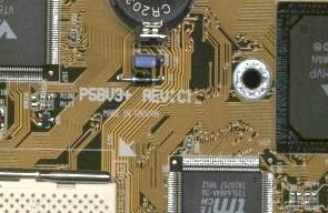
The revision number on the board. At the bottom left hand corner the processor bases, above the CMOS battery.
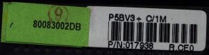
The board revision on the sticker on the outermost ISA plug
During introduction on the market summer ' 98 there was only the P5BV3+ Rev. A (for upgraders with old PS/2 memory modules) and Rev. B (with 3 DIMM slots).
Toward the end of '98 the Rev. B was introduced with slight changes as Rev. C, and later as fully K6-III compatible version K6BV3+ and in the ATX version K6XV3+. At end 1999 / beginning 2000 following boards K6XV3+/66 and K6BV3+/66 were released.
Beyond that there are still some exotic versions, the DFI site is occasionally referring to them.
The most important differences of the 7 type versions of the DFI P5BV3+:
| Version | RAM banks | Card slots | Dimensions | K6-CPU's | Remarks |
|---|---|---|---|---|---|
| P5BV3+ Rev.A | 2 PS/2, 2 DIMM Max. 256Mb |
1 AGP, 4 PCI, 3 ISA (1 shared) |
25x22 | All K6-2 K6-III 400 |
First version. All K6-2 types, K6-III 400 |
| P5BV3+ Rev.B | 3 DIMM Max. 384Mb |
1 AGP, 4 PCI, 3 ISA (1 shared) |
25x22 | All K6-2 K6-III 400 |
Version without PS/2. All K6-2 types, K6-III 400 |
| P5BV3+ Rev.C | 3 DIMM Max. 384Mb |
1 AGP, 4 PCI, 3 ISA (1 shared) |
25x22 | All K6-2 K6-III 400 |
Like Rev. B. The Jumper for the type of power connector (AT/ATX) is missing. |
| K6BV3+ Rev.A | 3 DIMM Max. 768Mb |
1 AGP, 4 PCI, 3 ISA (1 shared) |
25x22 | All K6-2 All K6-III |
1-2Mb Cache. Improves voltage supply for CPU and AGP |
| K6BV3+/66 Rev.B | 3 DIMM Max. 768Mb |
1 AGP, 4 PCI, 3 ISA (1 shared) |
25x22 | All K6-2 All K6-III |
Like K6BV3+Rev.A, with UltraDMA66, with voltage supply 1.30V-2.05V, 97MHz bus clock for K6-2-533 |
| K6XV3+ Rev.A | 3 DIMM Max. 768Mb |
1 AGP, 4 PCI, 3 ISA (1 shared) |
30x18 | All K6-2 All K6-III |
ATX board, 1-2Mb Cache, improves voltage supply for CPU and AGP |
| K6XV3+/66 Rev.B | 3 DIMM Max. 768Mb |
1 AGP, 4 PCI, 3 ISA (1 shared) |
30x18 | All K6-2 All K6-III |
Like K6XV3+Rev.A, with UltraDMA66, with voltage supply 1.30V-2.05V |
| P5BV3+/e Rev.A | 2 DIMM Max. 256Mb |
1 AGP, 3 PCI, 2 ISA (1 shared) |
20x22 | All K6-2 K6-III 400 |
Shorter than the other boards, Processor does not block long plug-in cards. (except AGP?) |
| P5BV3+/e Rev.B | ?? | ?? | ?? | ?? | Only BIOS updates available. |
The Jumper and switch positions/meanings unfortunately change from type to type. So far the meanings depend however not on the revision.
Most processor settings are made on one (AT boards) or two (ATX boards) DIP Switches. Altogether there are 10 or 11 switches, depending upon version:
| P5BV3+, K6BV3+ Rev.A: | SW1 1-10 |
| K6XV3+ Rev.A: | SW1 1-10, Jumper 8 |
| K6BV3+/66 Rev.B: | SW1 1-4, SW2 1-6 |
| K6XV3+/66 Rev.B: | SW1 1-5, SW2 1-6 |
The Switches are used mostly identically however. I use therefore in the following uniform way of writing:
| Board clock | Multiplicator | Processor power | |
|---|---|---|---|
| Way of writing: | xxx- "switch 1-3" |
-xxx- "switch 4-6" |
-xxxx or -xxxxx
"switch 7-11" |
| P5BV3+, K6BV3+ Rev.A | SW1 1-3 | SW1 4-6 | SW1 7-10 |
| K6XV3+ Rev.A | SW2 1-3 | SW2 4-6 | SW1 1-4 |
| K6BV3+/66 Rev.B | SW1 1-3 | SW1 4-6 | SW1 7-10, Jumper 8 |
| K6XV3+/66 Rev.B | SW2 1-3 | SW2 4-6 | SW1 1-5 |
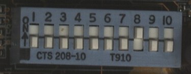
SW1 of a P5BV3+ with setting 000-000-0100 (100x3.5, 2.2V)
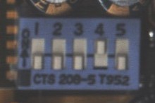
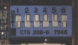
SW2 and SW1 of a K6XV3+/66 with setting 011-110-00010 (66x2.5, 2.8V)
Meanwhile in the manuals the multiplicators and the powers are documented. Nevertheless I here still specify them. The partial still undocumented FSB clock rates are further marked by (u). AMD constantly developed the K6 processor line further. Unfortunately such a change of generations causes nevertheless again and again difficulties to the boards.
The P5BV3+-Linie was layed out particularly to the K6-2 and appeared the same time with the K6-2. Which also required the first change of the board: The first board series ("A0") did not know the 95-MHz-clock for the K6-2-333 yet.
The next large step was the K6-III. With version 3 the K6 got a 256K large internal L2-Cache. running with processor clock (the L2-Cache of the board becomes thereby the L3.)
AMD introduced silently a revised processor design before, without the cache, as replacement for the normal K6-2. This processor is known as K6-2 CXT.
Still it is a vague announcement: AMD wants to present at the beginning of 2000 another further processor in the K6-Linie: The K6-2+ with 128K Cache.
The K6-2 CXT
The K6-2 CXT is, as said, only the early version of the K6-III. Probably the original K6-2-Design had stability problems, which made the change necessary starting from 350MHz.
With the K6-2 CXT two important details change:
- The multiplicator x2 is redefined to x6. Thus the processor on old boards can be operated as 66x6=400MHz. The upper border of the processor Design is accordingly with 100x6=600MHz.
- The K6-Feature "Write Allocation" is now differently switched on. That has unfortunately as a consequence that the BIOS must recognize and differently initialize this processor. An BIOS update is thus necessary, otherwise one does loose a few percent speed.
The normal K6-2
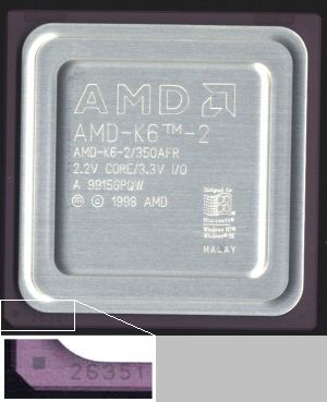
The K6-2 CXT. The number of 26351 is unfortunately badly readable.
The CPUID identification can be picked with e.g. ctcm of the C't. The current version determines also under "Write Strategie L1" whether the Write Allocation is activated:
PROZESSOR-
und CACHE-INF
c't 5/98/ Andreas Stiller V1.6n Prozesso
Timing : am6k86
Prozesso CPUID : AuthenticAMD Typ=00 Fam=05 Mod=08 Rev=0C Feat=008021BF
Prozesso Nam : AMD K6-2 Step 12
AMD 6k86 Konfig. :WCDE= false, WA-Limit= 0 MByte, WA-Hole 15Me= false
Aktueller Takt : 350.914 MHz, gemäß Pentium Timer:350.830 MHz
Primär-Cache (L1) : 32 KByte,2fach assoziativ
Sekundär-Cache (L2) :1024 KByte,direct mapped
Code Cache (L1) : 32 KByte,2fach assoziativ
Hauptspeiche : 64 MByte,kein Memory holes gefunden
Cacheable Area L1 : 64MByte, kein noncacheable Areas gefunden
Cacheable Area L2 : 64MByte, kein noncacheable Areas gefunden
Write Strategie L1 : Write Back, Write Allocation, linear Fill
Write Strategie L2 : Write Thru, no L2 Flush (wbinvd)
What I know so far about the DFI BIOS:
- The BIOS of 02.09.98 (09/02/98) does not support the K6-2 CXT yet.
- The BIOS of 26.11.98 (11/26/98) activates apparently the K6-2 CXT correctly.
- According to Q&A of DFI the K6-2-400 is supported starting from BIOS version of 12/15/98.
- On the web pages of DFI all processors up to the K6-III-550 are indicated now.
To the owners of a K6-2 CXT or K6-III: Ask mail to me: Is the processor initialized correctly? (examine with SetK6v3 of the C't whether the Write Allocation is correctly activated!) (request also to BIOS Versionsnummer/Datum send.)
The K6-III
The K6-III is essentially a K6-2 CXT with additionally 256K L2-Cache in the processor with full CPU clock. Thus unfortunately requirements of electric current of the processor increase clearly. Additionally the most K6-III's need (however not all!) a power of 2.4V, in order to function with the high clock frequencies stable. The 0.25µ production process of the K6-III is reaching slowly its clock limit...
With this the K6-III has a serious problem: Together with current-hungry high end 3D cards (in particular Voodoo 3) is often overstraining the 3.3V power supply of current boards. (with normal AT power the board produces the 3.3V from the 5V supply. ATX power already supplies 3.3V to the board)
Unfortunately the current supply of the entire P5BV3+-Linie is too weak in order to operate a K6-III starting from 450 MHz. These problems have forced DFI to release the P5BV3+-Linie only up to the K6-III-400. (the K6-2 is not so far concerned)
The faster K6-III's starting from 450MHz runs officially only on the new K6BV3+-Linie, which got a stronger 3.3V power supply.
In practice it showed up that the K6-III's to 450MHz functions perfectly even on older DFI boards.
Who has experience with K6-III's starting from 450MHz on a P5BV3+: Please mail!
The K6-2+/K6-III+
After last knowledge it will only be available for notebooks:: The K6-2+. Nevertheless one can operate this CPU probably in a normal board, presupposed, one gets one.
In order to be able to keep up in the Low Cost segment better, the K6-III-Design had to become more cheap. AMD tries to by reduction to 128K L2-Cache, shrinking the chip size, lowering the costs. The fact that "only" 128K Cache does not slow down the processor shows Intel with the Celeron impressively. And: Still a large L3-Cache stands for the K6-2+ to the side, so that the K6-2+ will be only insignificantly slower probably, as the K6-III.
Additionally AMD wants to also shrink the K6-2+ from 0.25µ to 0.18µ, which makes higher clock rates and lower current consumption possible. Unfortunately this advantage has a serious disadvantage:
With 0.18µ processors the operating voltage is usually with 1.5-1.6V. Rumor is that it is 1.9V-2.0V. The presently available boards, including all DFI-Socket7-Boards before the K6*V3+/66 board, supply 2.0V as smallest power!
AMD will also not give higher clock multiplicators than x6 to the K6-2+, with 600MHz the end of the K6's is reached. Here are the most interesting "undocumented" results to find. During the revisions A1, B5 and c1 of the board 2 switching positions were undocumented. They provide a 68.5MHz setting (34MHz PCI, 68.5MHz AGP) and a further 75MHz-setting also (37.5MHz PCI, 75MHz AGP) over-clocked.
According to enclosing note to my A1 the DFI supports since Rev. "A00+" 95 MHz board clock for the K6-2-333. What happens during older revisions with the 95-MHz setting, I cannot say. The K6XV3+/66 does not start with the undocumented switching positions unfortunately.
The K6BV3+/66 knows 97MHz for the K6-2-533 as the first board also. Strange to say DFI for it planned however a new Jumper.
It is well possible that the undocumented positions are once differently occupied sometime, e.g. with a 112MHz setting. Before one selects such a position, it is a good idea to set the multiplicator to 2.5 and check the processor clock with a diagnosis Tool, e.g.. ctcm of the C't.
(indication of MHz on boot is often wrong with unusual combinations)
Someone having a board revision with other clocks: Mail to me!
The PCI/AGP divisors are examined by speed measurements for correctness.
For all curious ones: The best method of the measurement is to couple the memory clock to the AGP clock and measure the memory throughput. The memory throughput is linear dependent on the clock, in contrast to the PCI/AGP transfer rate, which is slowed probably still by other bottle necks. And since I am repeatedly asked: SiSoft Sandra measures bullshit on 100MHz-Sockel-7 systems. Rather use ctcm.
| FSB clock | switch 1-3 | JP8 ** | AGP clock | AGP divisor | PCI clock | PCI divisor |
|---|---|---|---|---|---|---|
| 60 | 111 | 1-2 | 60 | /1 | 30 | /2 |
| 66 | 011 | 1-2 | 66 | /1 | 33 | /2 |
| 68.5 (u) | 101 | 1-2 | 68.5 | /1 | 34.25 | /2 |
| 75 (u) | 001 | 1-2 | 75 | /1 | 37.5 | /2 |
| 75 | 110 | 1-2 | 60 | /1.25 | 30 | /2.5 |
| 83 | 010 | 1-2 | 66 | /1.25 | 33 | /2.5 |
| 95 * | 100 | 1-2 | 63.3 | /1.5 | 31.65 | /3 |
| 97 ** | 100 | 2-3 | 64.67 | /1.5 | 32.33 | /3 |
| 100 | 000 | 1-2 | 66 | /1.5 | 33 | /3 |
** only K6BV3+/66
(u) undocumented. Only with P5BV3+ confirms. Not used with K6XV3+/66
With the K6-2 CXT and with the K6-III the multiplicator x2 was replaced by x6. Further to the K6-2 and to the K6-III above
| Switch 4-6 | AMD K6, K6-2 | AMD K6-2 CXT, K6-III | IBM/Cyrix M2 | IDT WinChip C6 | Intel Pentium | Intel Pentium MMX |
|---|---|---|---|---|---|---|
| -100- | 2 | 6 | 2 | 2 | 2 | 2 |
| -110- | 2.5 | 2.5 | 2.5 | 2.5 | 2.5 | |
| -010- | 3 | 3 | 3 | 3 | 3 | 3 |
| -000- | 3.5 | 3.5 | 3.5 | 4 | 1.5 | 3.5 |
| -101- | 4 | 4 | 4 | |||
| -111- | 4.5 | 4.5 | ||||
| -011- | 5 | 5 | 5 | |||
| -001- | 5.5 | 5.5 |
With the K6*V3+/66-series an additional switch was introduced, the powers made possible from 1.30V to 2.05V in 0.5V-steps.
Jumper JP5, (with Rev. A /e JP3) turns the Split Voltage support on: With 1-2 VIO=3.3V, with 2-3 is VIO=VCore. VCore is always the value between 2.0V and 3.5V set by the switches.
The processor pin VCC2DET, which should normally activate split voltage, is not evaluated.
The "old" powers: (with K6BV3+/66 set JP8 to 1-2!)
| Core power | switch
7-10/(7-11) * |
Jumper JP5 (A /e: JP3) |
Measured: | |
|---|---|---|---|---|
| Vcore | VIO | |||
| 2.0 V | -0000(0) | 1-2 | 2.05 V | 3.35 V |
| 2.1 V | -1000(0) | 1-2 | 2.15 V | 3.35 V |
| 2.2 V | -0100(0) | 1-2 | 2.25 V | 3.35 V |
| 2.3 V | -1100(0) | 1-2 | 2.35 V | 3.35 V |
| 2.4 V | -0010(0) | 1-2 | 2.46 V | 3.35 V |
| 2.5 V | -1010(0) | 1-2 | 2.56 V | 3.35 V |
| 2.6 V | -0110(0) | 1-2 | 2.66 V | 3.35 V |
| 2.7 V | -1110(0) | 1-2 | 2.76 V | 3.35 V |
| 2.8 V | -0001(0) | 1-2 | 2.85 V | 3.35 V |
| 2.9 V | -1001(0) | 1-2 | 2.95 V | 3.35 V |
| 3.0 V | -0101(0) | 1-2 | 3.05 V | 3.35 V |
| 3.1 V | -1101(0) | 1-2 | 3.15 V | 3.35 V |
| 3.2 V | -0011(0) | 1-2 | 3.26 V | 3.35 V |
| 3.3 V | -1011(0) | 2-3 | 3.36 V | 3.36 V |
| 3.4 V | -0111(0) | 2-3 | 3.46 V | 3.46 V |
| 3.5 V | -1111(0) | 2-3 | 3.56 V | 3.56 V |
The new powers of the K6*V3+/66: (with K6BV3+/66 set JP8 to 2-3!)
| Core power | switch 7-11, (Jumper JP8) * |
Jumper JP5 |
|---|---|---|
| 1.30 V | -0000(1) | 1-2 |
| 1.35 V | -1000(1) | 1-2 |
| 1.40 V | -0100(1) | 1-2 |
| 1.45 V | -1100(1) | 1-2 |
| 1.50 V | -0010(1) | 1-2 |
| 1.55 V | -1010(1) | 1-2 |
| 1.60 V | -0110(1) | 1-2 |
| 1.65 V | -1110(1) | 1-2 |
| 1.70 V | -0001(1) | 1-2 |
| 1.75 V | -1001(1) | 1-2 |
| 1.80 V | -0101(1) | 1-2 |
| 1.85 V | -1101(1) | 1-2 |
| 1.90 V | -0011(1) | 1-2 |
| 1.95 V | -1011(1) | 1-2 |
| 2.00 V | -0111(1) | 1-2 |
| 2.05 V | -1111(1) | 1-2 |
| Switch 1-3 | JP8 | 2* -100- |
2.5 -110- |
3 -010- |
3.5 -000- |
4 -101- |
4.5 -111- |
5 -011- |
5.5 -001- |
6** -100- |
|
|---|---|---|---|---|---|---|---|---|---|---|---|
| 60 | 111- | 1-2 | 120 | 150 | 180 | 210 | 240 | 270 | 300 | 330 | 360 |
| 66 | 011- | 1-2 | 133 | 166 | 200 | 233 | 266 | 300 | 333 | 366 | 400 |
| 68.5 (u) | 101- | 1-2 | 137 | 171 | 205.5 | 240 | 274 | 308 | 342.5 | 377 | 411 |
| 75 | 110- (001-) | 1-2 | 150 | 187.5 | 225 | 262.5 | 300 | 337.5 | 375 | 412.5 | 450 |
| 83 | 010- | 1-2 | 166 | 208 | 250 | 292 | 333 | 375 | 416 | 458 | 500 |
| 95 | 100- | 1-2 | 190 | 237.5 | 285 | 332.5 | 380 | 427.5 | 475 | 522.5 | 570 |
| 97*** | 100- | 2-3 | 193.8 | 242.3 | 290.7 | 339.1 | 387.6 | 436.1 | 484.5 | 533 | 581.4 |
| 100 | 000- | 1-2 | 200 | 250 | 300 | 350 | 400 | 450 | 500 | 550 | 600 |
** not with the K6, K6-2
*** only with the K6BV3+/66
Repeated occupying by IRQ's (IRQ sharing) should actually work with all PCI/AGP cards problem-free. It does not however. The more important it is to know how one can distribute the IRQ's manually. Here an overview of the IRQ's of the DFI boards:
| Fixed IRQ numbers | Allocation | Status |
|---|---|---|
| IRQ 0 | Timer | Fixed |
| IRQ 1 | Keyboard | Fixed |
| IRQ 2 | Cascaded IRQ | Fixed |
| IRQ 3 | Serial 1 | Can be disabled |
| IRQ 4 | Serial 2 | Can be disabled |
| IRQ 5 | Free | |
| IRQ 6 | Floppy disk | Fixed |
| IRQ 7 | Parallel 1 | Can be disabled |
| IRQ 8 | Realtime clock | Fixed |
| IRQ 9 | Free | |
| IRQ 10 | Free | |
| IRQ 11 | Free | |
| IRQ 12 | PS2-Mouse | If connected |
| IRQ 13 | Coprocessor | Fixed |
| IRQ 14 | IDE 1 | Can be disabled |
| IRQ 15 | IDE 2 | Can be disabled |
| Variable IRQ's | Allocation | Status |
| INT A | Main IRQ PCI 1 | |
| Main IRQ AGP | Can be disabled | |
| INT B | Main IRQ PCI 2 | |
| INT C | Main IRQ PCI 3 | |
| INT D | Main IRQ PCI4 | |
| USB Controller | Can be disabled | |
| ACPI | ACPI Controller | Can be disabled |
Old ISA cards occupy additional IRQ's, which one should register for problem recovery in the Setup. Onboard components use their IRQ's only, if they are active. In addition, occasionally even switched off equipment can disturb its IRQ line...
The IRQ numbers still free are distributed under the Plug n ' Play cards: Plug n ' Play ISA cards occupy their IRQ's exclusively. At the end the 4 PCI IRQ lines INT A - INT D will be distributed on the remaining IRQ numbers. (often 9 10 11 and maybe 5.) If less than 4 IRQ numbers are free, several PCI IRQ's are assigned to one IRQ number. ACPI uses a further IRQ from the PCI IRQ pool, this is however not directly connected with a PCI IRQ.
Note: The PCI Slot 1 uses always the same IRQ as the AGP Slot, the PCI Slot 4 always uses the same IRQ as the USB Controllers, if it is active. These IRQ lines are simply electrically connected.
PCI sound cards occupy often 2 IRQ's, from which however only one is a PCI IRQ, the other one serves the sound blaster emulation. Since this IRQ is only simulated, it can be assigned independent of the PCI IRQs, like for PnP ISA cards.
With PCI/AGP cards that use more than one IRQ, or that will not use their first IRQ, its unfortunately more complicated. See in addition C't 11/2000, s. 258. Some will have already noticed: The processor temperature is differently indicated in the Setup and with the Windows monitoring Tool. The error seems to be in the Windows program, since one gets with the help of a program for the CPU Powermanagement the processor (according to program) up to 3 degrees more coldly than the room air!
The current monitoring application for Win95 and WinNT can be downloaded under http://www.genesyslogic.com.tw/drivers_utilities/drivers.htm. Up to the version 1.22 the accuracy did not improve however. But the new version indicates also the power to VCore, unfortunately perfectly wrongly. For me it always indicates 2,47 V, independently of the adjusted power. The current version of 6.9.1999 seems to finally correctly measure however.
The current K6*-Boards received another revision of the monitoring chip, which is incompatible to the older monitoring Tool versions. On the bundled CD should however a functioning version be present. (for me an unknown version with sysmon.exe of 19.7.1999)
Linux friends do not go out empty: Under http://www.lm sensors.nu there is a universal hardware monitoring system for Linux for Download. The correct driver is "Genesys Logic GL518SM".
On the board is still another CPU fan connector with a Detect line for the fan RPM. Who looks for such a fan, patience must prove. Hardly a dealer offers such.
It is worthwhile itself to look at the available fans once more near: Possibly it turns out that the "normal" fan without the adaptor cable is exactly the needed.
If the processor became cold enough, the board switches the fan power off. That was not initially anywhere documented, functioned however nevertheless very well. The RPM monitoring is also intelligently enough to not strike alarm. Only exception: If the Windows Tool runs, the fan remains on. Windows 98 can use several graphics cards at the same time. The problem: Normally PCI cards have a higher priority, than AGP cards, i.e. the AGP card becomes automatically the secondary monitor.
The current BIOS versions have therefore a set UP option "INIT display first" (PCI/AGP), under "Integrated Peripherals", with which the priority can be turned around. On the web pages one does not find anything on it, but the DFI BIOS has an integrated SDMS BIOS of the version 3.06. The newer BIOSse of the K6*-Boards has even a SDMS BIOS of the version 4.03.02, with own SCSI Setup.
The SDMS BIOS extension allows booting of SCSI disks on BIOS free NCR/Symbios SCSI Controllers, e.g. the NCR810.
Naturally one can select also with the DFI whether one wants from IDE or SCSI boots... With all quality, no board is error free. And so also the P5BV3+ has occasionally its problems. The following Incompatibilities are well-known, which all relate directly to the board:
Board driver
First question for problems of the board: Are the board drivers up to date? Even the drivers of Windows 98 SE are not sufficient for a stable use. In extreme cases already the installation of Win98SE can fall, there a hardware component (very much liked: SCSI cards) without Via drivers simply does not function. Remedy: If somehow possible, install without this card. (start installation from hard disk?)
The newest versions are available at any time from VIA. It is enough to load the 4-in-1 driver, it contains all necessary single drivers.
Memory problems
PC100-Module at lowest price are often not from best quality. Additionally the DFI boards are quite discriminating with the selection of the modules. It is not unusual that certain modules function only in some boards.
Memory problems express themselves in instabilities and boot problems (more or less continuous beep tone).
Remedy for memory problems: Couple the RAM clock to the AGP clock (JP4), or set the bus clock under 100MHz. Or naturally use different memory modules.
Windows 95 & K6-2
Windows 95 (not 98) has a problem with the K6-2 starting from 350MHz, by which it comes to problems with the Windows start. (protection fault in IOS)
There is a Patch from Microsoft. Faster it can be found however at AMD. (why probably?)
What not everyone knows: There is an older version of this Patches, which functions on Win95b+USB/AGP-Patch only to 450MHz. The old version is to be recognized by the file C:\WINDOWS\SYSTEM\VMM32\NTKERN.VXD version 4.03.1212. The newer version is 4.03.1213.
BIOS update
Normally BIOS updates are not a problem. One frequent question is whether to flash all in-between versions: This is not necessary. Just flash the latest version.
Important: Always use the Flash programm provided to the BIOS! Also when flashing an older version! In particular the Flash programm of the Jan-2000 bios does not seem to get along with the older BIOS files.
Wenn's is already too late, you may get a black screen after the reset. In this situation one can start the BIOS however possibly still from a boot disk and ' in the blind flight ' flashing. Good luck!
IBM disks
The P5BV3+ Rev.A and Rev.B has problems with IBM disks of the DTTA series. (much liked for the cheap 10GByte versions)
The disks are occasionally not recognized on boot, whereby the computer does not boot or boots from the second disk. The problem is fixed starting from Rev. C. Who does not disturb itself at an occasional starting problem however, the disk can be used without problems.
Graphics cards
The P5BV3+-Line had a too weak voltage supply at the AGP slot. Extremely hungry grahics cards can cause voltage supply overloads. Riva TNT(2) cards and Voodoo3 cards do work, GeForce cards can cause problems however. There is a solution from Friedrich Sperzel
TV cards
With some Broketree based TV cards (in particular Miro PCTV) it comes to different crashes, if DirectX based Capture software (TV software, videotex Dekoder...) is running. (particularly diskette accesses/sound card use)
Some problems disappear, if one disables the CPU to PCI Write Buffer in the chip set feature setup. According to DFI that does not affect the performance...
There are irregular problems also with Video+disk activity, which disappear, if one does without the VIA bus master drivers.
FritzCard PCI
With the FritzCard PCI there are partial of crashes when accessing the card. Remedy again: Disable the CPU to PCI Write Buffer in the chip set feature Setup.
PC66-memory in K6*V3+-Boards
Some BIOS revisions come into trouble, if a PC66-memory module with EEPROM is found.
IDE CD burner
Actually a problem of the Via Chipset and the Via driver: IDE CD burners often do not work with the DMA mode of the disk drivers clearly.
Remedy:
- Old drivers: Driver Setup start, option Enable/Disable DMA select and disable the DMA mode of the burner.
- New drivers: Together with the drivers a program was installed "VIA DMA Tool". There is a switch to turn off the DMA mode of the burner.
Memory size
From today's view the maximum memory size is a very much more interesting question, than from the view of 1998.
The P5BV3+ board supports, like suggested above, only memory modules with maximum of 128Mb capacity. The K6BV3+ and K6XV3+ board also support modules with 256Mb. However not every module of this capacity is supported, for the maximum size special modules are necessary with a high number (16 or 32) of chips. Modules with 3 or 8 chips are recognized with smaller capacity.
Unfortunately the memory size is further limited: The external Cache covers only parts of the main memory, and apart from the II+ and III+ processors a size beyond this border is not a good idea.
Here the maximum cached memory, dependent on the Cache size:
| Cache | Max memory |
| 512k Write back | 64Mb |
| 512k Write Through | 128Mb |
| 1Mb Write back | 128Mb |
| 1Mb Write Through | 256Mb |
| 2Mb Write back | 256Mb |
| 2Mb Write Through | 512Mb |
From today's view this memory size seems ridiculously small, in 1998 it was enormous.
A further popular hurdle: Windows 9x/ME only supports up to 512Mb main memory, there's no point in using more than that.
Manuals, Bios and drivers
They're still available: Manuals, drivers and BIOSse are to be found on www.dfi.com in the Download area. Since the last BIOS versions were not tested intensively any longer, they are to be found only in the beta section, though they work without problems!
PCI revision
Some modern PCI cards, in particular wlan cards, point out in the product description explicitly that they are PCI-2.2 cards. Normally this means that the card requires 3.3V power supply at the PCI slot, which was still optional with PCI-2.1. As far as I know, no board of the P5 and K6 series provides 3.3V supply at the PCI plug, therefore such cards do not work.
Disk capacity
The last official BIOS versions of the P5 and K6-Boards support only disks up to 32Gb. Larger disks are not recognized. The last beta BIOS fixes this. These are not not generally worse, they are just less well tested by DFI. With the update the likely next hurdle is the 128Gb limit. Also Windows 9x/ME/NT does not support disks largr than 128Gb.
Overclocking beyond 100MHz
Who simply cannot leave it: With BIOS editors one can produce modified BIOSse, which make bus clocks possible beyond of 100MHz, and with it the processor can be overclocked over the 600MHz border. Some CPU tools can increase the bus clock also while running, and need no special BIOS. After next boot the original setting of the jumpers is active again.
ATX short-circuit
An report reached me that on a P5BV3+ Rev.C the 5V line and the 5VSB line is short circuited, and the 5V Standby supplies the normal 5V supply while switched off. This can cause problems with the power supply and with disks etc.. Whether this concerns all boards and whether there is a connection to the (missing) ATX Jumper, is unclear.